
A binary storage cell storing 1 bit of information can be obtained from SR latch with gates , which is an electronic circuit made with transistors .
This semiconductor memory / RAM can be of 2 types :
SRAM: Static Random Access Memory.
binary values are stored using flip-flop constructed of transistors. A static RAM will hold its data as long as power is supplied to it.
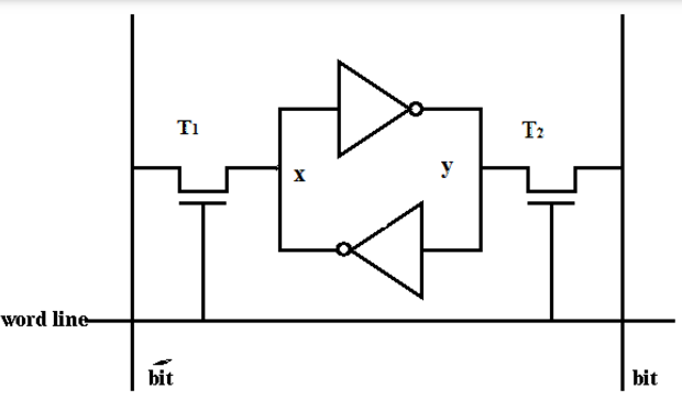
Transistors are cross connected . states are stable as long as the dc supply voltage is applied.
DRAM: Dynamic Random Access Memory.
store data as charge on capacitors.
capacitors have a natural tendency to discharge due to leakage current, dynamic RAM require periodic charge refreshing to maintain data storage.
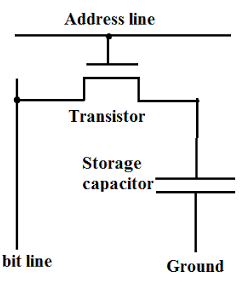
write operation, a voltage signal is applied to the bit line ( 1 high , 0 low ) . signal is applied to to the address line, which will turn on the transistor T, allowing a charge to be transferred to the capacitor.
read operation, when a signal is applied to the address line, the transistor T turns on and the charge stored on the capacitor is fed out onto the bit line B and to a sense amplifier , which compares the capacitor voltage to a reference value and determines if the cell contains a logic 1 or a logic 0. The read out from the cell discharges the capacitor
Circuits
2 main circuit classes are :
1. Combinational circuits
Combination Logic Circuits are made up from basic gates (AND, OR, NOT) or universal
gates (NAND, NOR) gates that are “combined” or connected together to produce more
complicated switching circuits.
- Circuits without memory
- Outputs depend only on current input values
example : Half adder,Full adder, Half subtractor, Full subtractor, Code converter, Decoder, Multiplexer,Demultiplexer, Encoder, ROM, etc.
2. Sequential Circuits (also called Finite State Machine)
Outputof a sequential logic device depends on its present internal state ( memory )and the present inputs.
- Circuits with memory
- Memory elements to store the state of the circuit
- The state represents the input sequence in the past
- Outputs depend on both circuit state and current inputs
Examples : Registers, Shift register, Counters etc.
Latches, Flip-Flops and Registers
devices to store information.
- – Latches and Flip-Flops – single bit
- – Registers – multiple bits
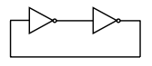
pair of cross coupled inventors store a binary state indefinitely , but cannot provide control logic .
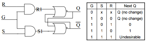
SR Latch (Basic Latch)
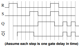
SR latch can act as a storage device (S : Set, R : Reset)
- – If R = 1 and S = 0, then Q goes to 0 and ‾Q goes to 1
- – If R = 0 and S = 1, then Q goes to 1 and Q goes to 0
- – If R = 0 and S = 0, then Q and Q remain where they are
- – If R = 1 and S = 1, then will not have a stable state
Next Q = R + Q
Next Q = S + Q
Gated SR Latch
Adding an enable control input G (sometimes called CLK)
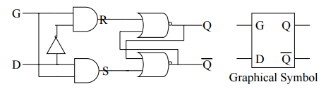
Gated D Latch
G acts as a control signal
– G = 0 means no writing, G = 1 allows writing
– The value written is that of input D
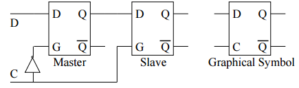
Master-Slave D Flip-Flop (D Flip-Flop)
Data is written in flip-flop when an edge of clock signal C arrived ( connected two gated latches)
When C is low, first latch gates data on D, second does nothing
• When C goes high, second latch latches what is Q of first latch
T Flip-Flop
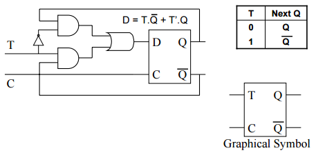
• Remain the same when T=0
• Toggle the state when T=1
JK Flip Flop
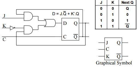
Combines the behaviors of SR and T Flip-Flops
• It behaves as the SR flip-flop where J=S and K=R (except J=K=1)
• If J=K=1, it toggles its state like the T flip-flop
